First testing of and changes to ESD generator
Posted on zo 04 oktober 2020 in NLnet
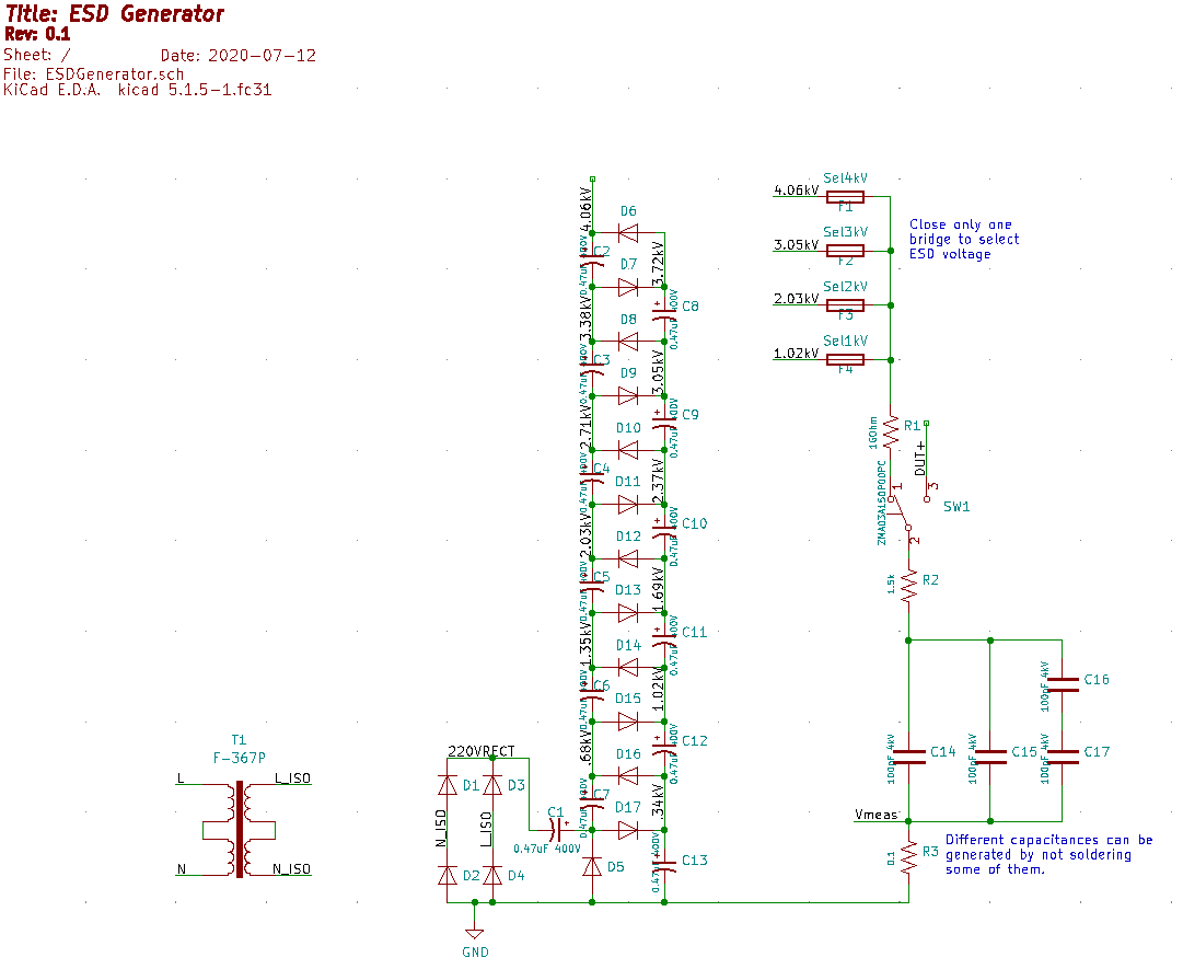
As reported in a previous blog post I am working on a small circuit to generate high voltages for some ESD testing. I now received the PCBs and the components for on the PCB and even did find some time to do the first testing of the design. As a reminder this is the schematic of the ESD generator:
To do the first testing I just populated the transformator, the diode bridge and components C1, C13, D5 and D17. This can be seen in the next picture:

It should allow to test if a voltage of 400V can be seen on C13 but unfortunaltely this is not the case. Testing reveals that it does not keep it's value.
In order to see if no design errors were made or maybe polarity of the diodes was switched, first the functionality of the diode bridge was checked. In the next image two oscilloscope snapshots are shown:


Here N_ISO was taken as 0V reference and L_ISO is shown in yellow on channel 1. Here a peak-to-peak voltage over 870V is seen which is higher than expected. For 240V AC a peak-to-peak voltage just under 680V is expected. I checked the transformer datasheet and verified I connected both primary and secondary in series. Multi-meter measurement confirms the increased voltage on the unloaded transformer: 244V AC on primary and 307V AC on secondary.
On the oscilloscope snapshots also on channel 2 in purple the board GND is shown on the left image and 220VRECT net on the right. This confirms that the board ground correctly follows L_ISO when the latter is below zero and 220VRECT follows it when above 0V. Switching reference voltage to the board ground gives then the following picture:

Here 220VRECT is shown as channel 1 in yellow and L_ISO on channel2 in purple. It confirms the correct working of the diode bridge. Next step is to measure the voltage on C13 which should keep the peak voltage stored due the diodes blocking reverse currents. This is given in the next oscilloscope measurements:


On channel 1 still 220VRECT is shown and on channel 2 now the voltage over C13 is given. On the left the original designed 150pF capacintance value for C1 and C13 was used and on the right both capacitances were doubled to 300pF. For the original capacitance value one can see that the value reaches only a maximum of 94V and decreases again, with doubling of the capacitances the voltages improve slightly. For safety, I used very small capacitors to limit the maximum current that this circuit can provide at high voltages. It seems I made it too small compared to the leakage current of the diodes. The rectified voltage was supposed to be 270V peak-to-peak oscillating at 100Hz, with a capacitance of 150pF this gives a maximum current of around 4µA with a capacitance of 150pF. Checking the diode datasheet gives a maximum leakage current of 5µA which is higher than the maximum current capability.
So the conclusion of this first experiment is that C1 has to be increased to have a maximum current significantly higher than the diode leakage current and also the storage capacitors like C13 need to increased to minimize the ripple on it's output caused by the diode leakage currents. I have now ordered a capacitor kit in order to experiment with different capacitance values.